
KB: Resolving Un-Routed Net Dead Copper DRC Violations
Solution Details
In Altium Designer, a DRC violation occurs when there is dead copper or zero-area regions or polygons on a PCB layer that is not assigned to any net. The error message appears as:
"Un-Routed Net Constraint: Region (0 hole(s)) <Layer Name> Dead Copper - Net Not Assigned."
The challenge arises when this dead copper is not visible in the PCB layout, making it difficult to locate and delete manually.
There are two primary methods to resolve this issue:
1. Using the PCB Health Check Monitor
2. Manual Removal via the PCB Rules And Violations Panel
1. Using the PCB Health Check Monitor
Altium Designer 22 introduced the Health Check Monitor functionality, which can automatically detect and fix zero-area polygons or dead copper. The functionality is only available for Altium Designer 22 and later versions.
Steps:
- With nothing selected in the PCB document open the Properties Panel.
- Click on the Health Check tab.
- Click Check All.
- Select the Zero Area Regions check.
- Click on Fix Issues to automatically delete zero area regions.
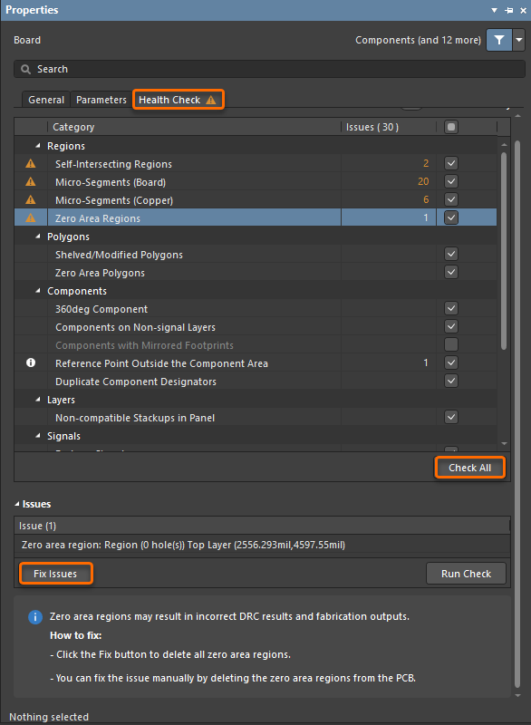
Health Check Monitor
2. Manual Removal via PCB Rules And Violations Panel
If using an older version of Altium Designer or preferring manual control:
Steps:
- Run the DRC: Tools » Design Rule Check... » Run Design Rule Check....
- Open the PCB Rules And Violations Panel.
- Ensure the Select option is enabled in the panel.
- Navigate to and select the UnRoutedNet rule.
- Select the "Dead Copper - Net Not Assigned" violation.
- Press Delete or use Edit » Delete to delete the dead copper.
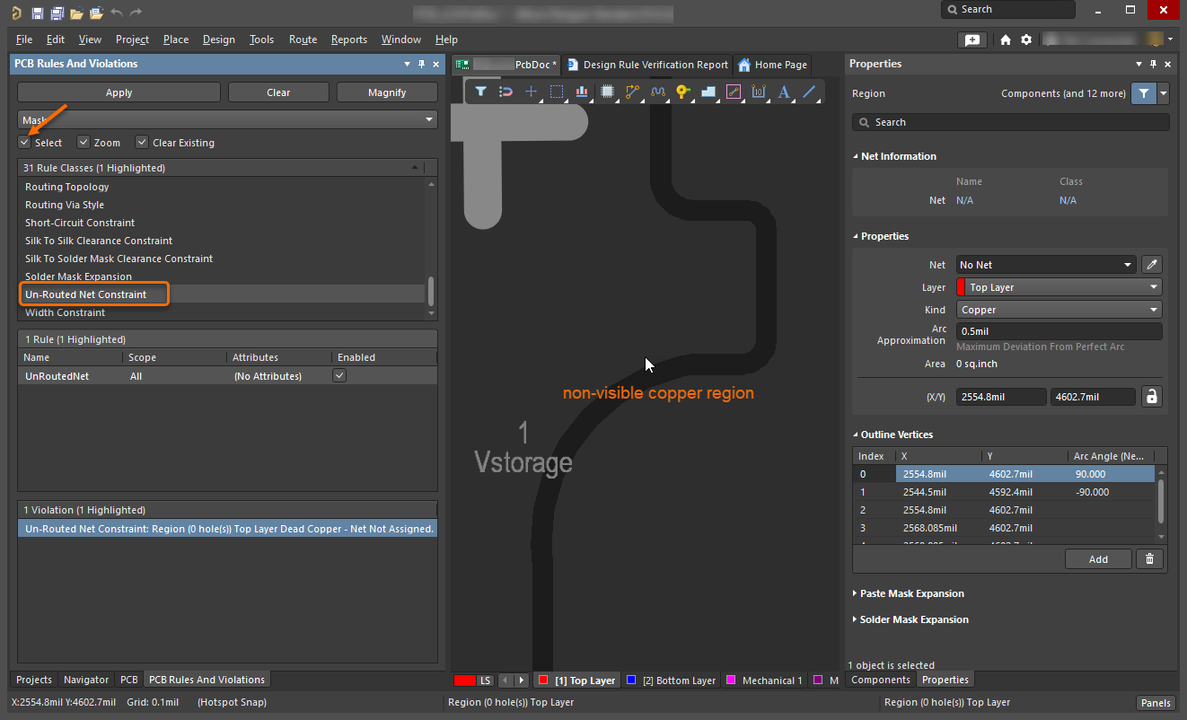
Rules And Violations Panel
Note: Dead copper and zero-area objects can further be inspected with the PCB List Panel:
Steps:
- Open the PCB List Panel.
- Check the Area Size and Layer of the suspected objects.
- Right-click and choose Zoom Selected to locate the objects on the layout.
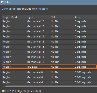
PCB List Panel