 Even the simplest board needs design detail beyond the tracks and pads that implement the circuit. It might be the board dimensions or the fabrication detail, it might be the component courtyards, or it might be the 3D component models. In Altium Designer, this type of additional information is detailed on Mechanical Layers.
Mechanical Layers and Component Layer Pairs
If the information being included on a mechanical layer is not related to a specific side of the board, for example, fabrication notes that detail the layer order, then an individual mechanical layer is added.
If the information is required on both sides of the board, for example the component courtyards, two mechanical layers are assigned: one layer holding the courtyard detail when the component is placed on the top side of the board; the other mechanical layer holding the mirror image of that same courtyard detail when the component is flipped to the bottom side of the board. In this situation, a pair of mechanical layers are added as a Component Layer Pair. When mechanical layers are added as a Component Layer Pair, they are displayed in the Component Layer Pairs section of the View Configuration panel, as shown below. Below that are the individual Mechanical Layers.

A number of user-defined Component Layer Pairs have been added.
| Display of Layer Pairs |
In the design space, the two layers in a Component Layer Pair are displayed on separate layer tabs using the naming Top <LayerPairName> and Bottom <LayerPairName> (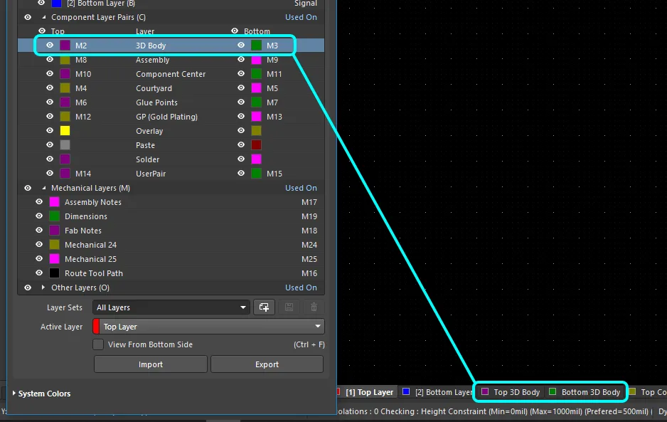 ). ).
|
| In the Library editor |
In the PCB library editor, additional design objects required in a component footprint are placed on the top layer of the Component Layer Pair. When the component is flipped to the bottom side of the board during PCB layout (L shortcut as a component is being moved), the contents of the top layer in the pair are automatically mirrored onto the bottom layer in the pair. |
| Automatic layer creation |
If a mechanical layer or a Component Layer Pair defined in the PCB library has the Layer Type assigned, that mechanical layer / layer pair is automatically created on the PCB when a component using those layers is placed. If the PCB already has a mechanical layer / layer pair of that Layer Type, the contents of those layers are mapped accordingly. |
Layers without
a Layer Type |
For mechanical layers / layer pairs defined in the PCB library that do not have a Layer Type assigned in the library, individual mechanical layers are created on the PCB. In this situation, pre-define the mechanical layer / layer pair in the PCB using the same layer numbers before placing the component, as the software will fall back to matching by Layer Number if it is unable to match by Layer Type. |
Adding Mechanical Layers to the Design
Mechanical layers are added, edited and removed in the View Configuration panel, as shown below. Their visibility and color are also configured in the panel. Use the  button at the bottom-right of the design space then select View Configuration, or press the
 L shortcut key to display the panel.
Right-click anywhere in the Layers region of the panel to display the context menu, providing commands to Add Component Layer Pair (a pair of mechanical layers) and Add Mechanical Layer (an individual mechanical layer).
 Individual or pairs of mechanical layers are added using the View Configuration panel right-click menu.
-
The mechanical layers / layer pairs can be sorted by name or by number in the View Configuration panel, configure this in the PCB Editor – General page of the Preferences dialog (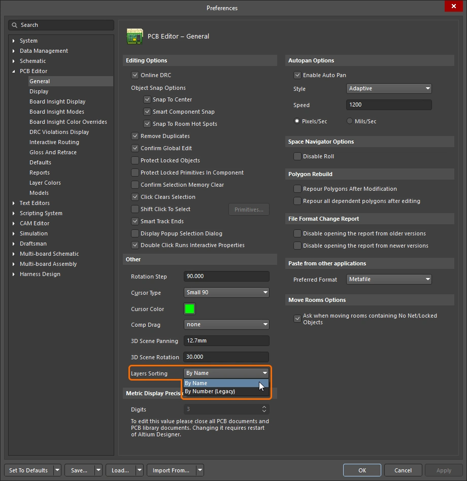 ).
).
-
When a via that has the via type set to IPC-4761 in its properties, new types of mechanical layers (Capping, Filling) and component layer pairs (Covering, Plugging, Tenting) are automatically added to the design, with corresponding shapes on these layers. The entries for these layers are shown in the View Configuration panel. Note that you cannot change the names and types of these layers, only their numbers.
-
There is no limit to the number of mechanical layers that can be added. Note that even though older versions of Altium's PCB design software are limited to 32 mechanical layers, newer PCB files that contain more than 32 layers can be safely opened and edited in an older version of the software.
Adding an Individual Mechanical Layer
When you select the Add Mechanical Layer command from the View Configuration panel right-click context menu to add an individual mechanical layer, the Edit Layer dialog opens.
 Configure the new mechanical layer.
Edit Layer dialog
|
| Layer Name |
Can be either a user-defined layer name, or system assigned if a pre-defined type is chosen in the Layer Type dropdown. If a pre-defined Layer Type is selected and then a user-defined name is entered into this field, the assigned Layer Type will appear within parentheses next to the user-defined naming on the View Configuration panel. |
| Layer Number |
The number of the mechanical layer that is being configured, the next-available layer number is offered. If another number is selected and it is already in use, a warning icon will appear ( ). An unused layer number will need to be assigned to continue. ). An unused layer number will need to be assigned to continue. |
| Layer Type |
The Layer Type can be unassigned (N/A), or you can select a type from the list. Available Layer Types are described below. |
Available Mechanical Layer Types
| Assembly Notes |
Often used to detail the component load order and/or important assembly instructions. |
| Board |
Use this layer for board-related instructions or details. |
| Board Shape |
Use this layer for the overall board outline (board shape).
-
When designing a PCB in advanced rigid-flex design mode, this mechanical layer type is automatically created to hold the primitives when a Board Region is converted to free primitives (Board Planning mode, Tools » Convert » Explode Region to Free Primitives).
-
As an alternative to defining the shape on a mechanical layer with a Layer Type of Board Shape, the Gerber standard supports the automatic generation of a board Profile fabrication file when the Gerber Board Profile is enabled in either the Gerber Setup or the Gerber X2 Setup dialog. This board profile is derived directly from the actual board shape, not objects placed on a mechanical layer with a Layer Type of Board Shape. Learn more about generating the Gerber Board Profile directly from the board shape.
|
| Dimensions |
Used to define the dimensional detail required for the board. |
| Fab Notes |
Used to detail important fabrication notes. |
| Route Tool Path |
Used to indicate the layer that contains the mechanical routing information. Note that a user-defined name is not permitted when using this layer type ( ). ).
|
| Sheet |
Use this layer to define the outer document drawing template border. See details in the Sheet Representation and Settings section below. |
| V Cut |
Used to define V cut details. V cuts are used to split circuit boards by cutting a "v" groove on the top and bottom of a circuit board while leaving a minimum amount of material in place to hold the panel of boards together. |
Adding a Component Layer Pair
When you select the Add Component Layer Pair command from the View Configuration panel right-click context menu, the Edit Layers Pair dialog opens.

Edit Layers Pair dialog
|
| Layer Name |
Can be either a user-defined layer name, or system assigned if a pre-defined type is chosen in the Layer Type dropdown. If a pre-defined Layer Type is selected and then a user-defined name is entered into this field, the assigned Layer Type will appear within parentheses next to the user-defined naming on the View Configuration panel. |
| Layer Number |
The numbers of the mechanical layers that are being configured, the next-available layer numbers are offered. If another number is selected and it is already in use, a warning icon will appear (). An unused layer number will need to be assigned to continue. |
| Layer Type |
The Layer Type can be unassigned (N/A), or you can select a type from the list. Available Layer Types are described below. |
Available Component Layer Pair Types
| Assembly |
Used to draw/detail assembly data for the component. This layer can be included in a Draftsman Board Assembly View, and can then be selected as the Geometry Source for the components in the Draftsman Component Display Properties dialog. Learn more about Draftsman. |
| Coating |
Used to define component areas that require a protective coating. |
| Component Center |
Used to indicate the centroid of the component, providing a visual reference of the location used by the component placement machine, in the assembly documentation. |
| Component Outline |
Used to define the outline of the component body, representing the area the component occupies on the board. |
| Courtyard |
Used to define the placement space required for a component. Typically the Courtyard will outline the component and pads, with a suitable clearance buffer (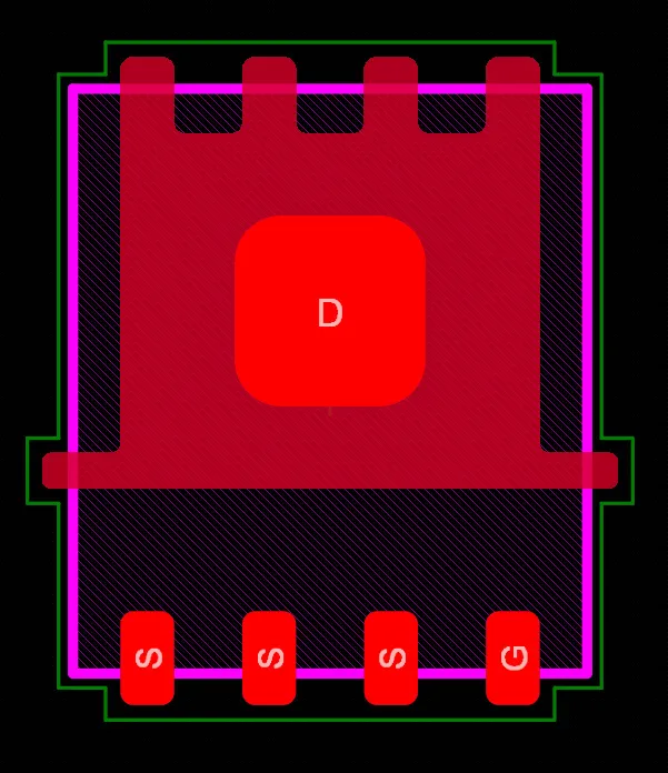 the green outline is the Courtyard). Learn more about Custom Footprint Creation. The shape defined on the Courtyard layer is also used for component selection, to define the component area, and for collision detection when there is no 3D Body included in the component. the green outline is the Courtyard). Learn more about Custom Footprint Creation. The shape defined on the Courtyard layer is also used for component selection, to define the component area, and for collision detection when there is no 3D Body included in the component. |
| Designator |
Use this layer to place the .Designator special string. This layer pair can then be included in assembly drawings that require the component designator to be displayed. Learn more about special strings. |
| Dimensions |
Used to define the dimensional detail required for components. |
| Glue Points |
Used to define component glue dots. |
| Gold Plating |
Used to define component selective gold plating requirements. |
| Value |
Use this layer to place the .Comment special string. This layer pair can then be included in assembly drawings that require the component value to be displayed. Learn more about special strings. |
| 3D Body |
Use this layer for the 3D mechanical model of the component. Learn more about 3D Body placement. |
| Die |
Use this layer for die pads and die 3D bodies when creating a Chip-on-Board component. Learn more about Wire Bonding. |
| Wire Bonding |
use this layer for bond wires when creating a Chip-on-Board component or directly in a PCB document. Learn more about Wire Bonding. |
Draftsman can define the outline of each component outline in a Board Assembly View based on the shape defined on the PCB Editor's Assembly component layer pair. Draftsman also supports including any mechanical or component layer pair, such as a Designator pair, in a Board Assembly View. These settings are defined in Draftsman's Properties panel when the Board Assembly View is selected. Learn more about Draftsman.
The Advantage of Assigning a Layer Type
A common approach to managing mechanical layer usage is to assign a dedicated layer number for each required mechanical layer function. This approach requires all designers to adhere to the same layer assignment and numbering scheme. It can also create difficulties when components are obtained from other sources that do not follow the same assignment and numbering scheme. If a different scheme has been used, the design objects must be moved from their current mechanical layer, to the mechanical layer assigned for that function.
This issue is resolved by assigning a Layer Type property. When a component is placed from a library into the PCB editor, or copied from one library to another, or created by the IPC Footprint Wizard, existing Layer Type assignments are automatically matched, regardless of the mechanical layer number(s) assigned to those Layer Types. The objects are relocated on the correct layer(s) according to their Layer Type. If the software is unable to match by Layer Type, it will fall back to matching by Layer Number.
For both individual mechanical layers and Component Layer Pairs, you can select a Layer Type from a pre-defined list of types. The images below show the list of available Layer Types. You can access the dialogs shown below by right-clicking on an individual layer, then selecting the Edit Layer or Add Component Layer command from the menu.

Select the Layer Type from the pre-defined list of Types; individual mechanical layers are shown on the left; Component Layer Pairs on the right.
Naming Layers with a Layer Type Assigned
When a Layer Type is assigned, the layer automatically has its Layer Name property changed to be the same as the Layer Type. This can be overridden, if needed, by typing in a user-defined name. When a layer has a user-defined name and a Layer Type assigned, both are displayed with the Layer Type shown in brackets, as shown below for the Layer Pair GP (Gold Plating).
 The Layer Type is used to name the layer, this can be overridden if required.
The Route Tool Path Layer Type
There is one exception to the naming behavior just described when a Layer Type is assigned – a user-defined name is not permitted when the Layer Type is set to Route Tool Path. The reason for this is that older versions of the software use the name of the Route Tool Path layer to identify the layer that contains the route information (also referred to as rout information). Fixing the naming of this layer ensures that the design will continue to function correctly in an older version.
The Route Tool Path layer type is used to indicate the layer that contains the mechanical routing information. A typical approach to using this layer is to place tracks and arcs around the outer edge of the board shape to define the machining path and width. Solid sections are left to hold the board within the panel, then a series of small holes are placed across each solid section to create perforations (often referred to as mouse-bites), allowing the board to be snapped out of the panel once the assembly process is complete.
When the board is displayed in 3D mode, objects detected on the Route Tool Path layer are displayed as a routed slot in the board, as shown below.
Objects detected on the Route Tool Path layer are used to visualize the routed board, in 3D display mode.
Use the Line/Arc Primitives from Board Shape dialog to trace the outside of the board shape with tracks and arcs (shown below). Enable the Route Tool Outline option in the dialog to have the objects placed outside the board shape rather than centered along its edge. Some designers prefer to add the fabrication information when they use the Embedded Board Array feature to create an assembly panel, rather than including this detail in the actual board file.

Learn more about Board Panelization using an Embedded Board Array
Defining the Layer Type in the PCB Library Editor
If a mechanical layer or a Component Layer Pair defined in the PCB library has the Layer Type assigned, that mechanical layer / layer pair is automatically created on the PCB when a component using those layers is placed. If the PCB already has a mechanical layer / layer pair of that Layer Type, the contents of those layers are mapped accordingly.
Where possible, it is recommended to edit the source library and assign Layer Types. When a component footprint is placed (or copied) from a library, mechanical layers and Component Layer Pairs of those Layer Types are automatically created in the target board (or library) if they do not exist. If those Layer Types already exist in the target board (or library), the layer contents are automatically mapped to the correct layer.
For mechanical layers / layer pairs defined in the PCB library that do not have a Layer Type assigned in the library, individual mechanical layers are created on the PCB. In this situation, pre-define the mechanical layer / layer pair in the PCB using the same layer numbers before placing the component, as the software will fall back to matching by Layer Number if it is unable to match by Layer Type.
Learn more about Handling Special Layer-specific Requirements in the PCB library editor
Working with Mechanical Layers
Mechanical layers are added, edited, deleted and displayed through the View Configuration panel in the PCB editor. They are not displayed or edited in the Layer Stack Manager.
Displaying
 Configure the visibility of layers in the View Configuration panel, and save commonly used sets of layers as a user-defined Layer Set.
| Controlling layer visibility |
Click the visibility icon ( ) next to the layer's name to toggle the display of that mechanical layer on or off. Alternatively, click to select the layer name and then press the ) next to the layer's name to toggle the display of that mechanical layer on or off. Alternatively, click to select the layer name and then press the Spacebar (this toggles the display of both layers in a Component Layer Pair). |
| Include in Single Layer Mode |
Mechanical layers have an additional display feature; they can be set to remain visible when the display is in Single Layer Mode. Hold Ctrl as you click on the visibility icon of a mechanical layer to enable the Display in Single Layer Mode feature – the visibility icon changes to indicate that this layer has this feature enabled ( ). ). Ctrl+Click a second time to disable this mode.
Single Layer Mode is a handy display control feature in which all other layers are hidden apart from the active (current) layer. Press Shift+S in the design space to cycle through the enabled Single Layer Modes. When the display is in single layer mode, the non-active layers can be completely hidden, set to gray, or set to monochrome. Learn more about Single Layer Mode.
|
| Include in 3D View Mode |
Mechanical layers can also be included in the 3D display, when the 3D Settings are enabling the Colors - By Layer option. Enable the option in the View Options tab of the View Configuration panel when the board is displaying in 3D View mode. The mechanical layers that are currently configured to be visible will be included ( ). ).
|
Controlling what is displayed in the editing space means lots of toggling layers on and off. An invaluable feature in helping in this process is to define your own Layer Sets, which you can quickly switch between using the  button at the bottom of the editing space.
Learn more about Layer Sets
Editing and Deleting
To edit the settings of an existing component layer pair or mechanical layer, double-click directly on its entry on the View Configuration panel (or right-click on the desired entry and choose Edit Layer from the context menu). Make changes in the Edit Layers Pair / Edit Layer dialog as required. The visibility and color of mechanical layers are configured directly in the View Configuration panel.
To delete a layer, you can right-click on the desired layer and select Delete Layer. Depending on how the layer is being used, there will be three outcomes:
| Nothing on the layer |
If there are no primitives placed on the layer, it is deleted immediately when you select Delete Layer (without confirmation). |
| Contains unlocked primitives |
If there are unlocked primitives on the layer, a pop-up will appear asking for confirmation of deletion. |
| Contains locked primitives |
If there are locked primitives on the layer, for example it contains primitives that belong to a component, an error pop-up will appear to alert you that the action cannot be completed. |
Exporting and Importing
The structure of mechanical layers and component layer pairs added to a PCB can be duplicated to another PCB by exporting that set into a file from the source PCB document and then importing the file to the target PCB document.
Export / Import the Layers
-
In the source PCB document where the required structure of mechanical layers and component layer pairs is added, use the Tools » Export Mechanical Layers command from the main menus. Use the Export Mechanical Layers dialog that opens to define the name and the directory for the *.stackup file that will contain data about the mechanical layer structure.
-
In the target PCB document, use the Tools » Import Mechanical Layers command from the main menus and use the Import Mechanical Layers dialog that opens to select the saved *.stackup file. The added structure of mechanical layers and component layer pairs can be seen in the View Configuration panel.
Copy / Paste the Layer Contents
Note that the Import/Export commands transfer the structure of mechanical layers and component layer pairs, they do not transfer the content of these layers.
To copy the content of:
-
A single mechanical layer, use the Edit » Select » All on Layer command when the required layer is the active layer in the source PCB, then use the standard copy/paste process to replicate that data in the target PCB.
-
Multiple mechanical layers, configure the layer visibility in the View Configuration panel to only display the required mechanical layers, then drag a select-touching rectangle (right-to-left) around all the required primitives in the source PCB, then use the standard copy/paste process to replicate that data in the target PCB.
Note that the active is not important during paste into the target PCB, primitives are automatically pasted onto the same layer that they were copied from.
Presentation and Output Settings
Mechanical layers are often used to detail information that needs to be included on printouts or generated fabrication output. This can include drawing templates, fabrication instructions, assembly instructions, and so on. If required, this can be done directly in the PCB editor.
 Board production documentation information can be included on mechanical layers, if required.
Alternatively, these documentation tasks can be performed in Draftsman, an advanced, flexible graphical editing environment for creating board design production documents. Complete with a dedicated set of drawing tools, the Draftsman drawing system provides an interactive approach to bringing together fabrication and assembly drawings with custom templates, annotations, dimensions, callouts, and notes.
Learn more about Draftsman
Sheet Presentation and Settings
The image above shows a white background that exactly fits the drawing objects placed to represent the sheet template. This is created by adding a mechanical layer with the Layer Type set to Sheet, which is then used to define the document drawing template outer border.
The size of this white background is defined by the Sheet Settings, which can be customized in the Properties panel when there is nothing selected in the editing space. The X/Y values of the sheet's bottom-left corner, and the Width and Height can be configured manually. Alternatively, when the Get Size From Sheet Layer option is enabled the sheet background is automatically calculated from the bounding rectangle of the set of objects placed on the Sheet Layer-Type mechanical layer.
 The sheet background can be sized automatically from the objects placed on the Sheet Layer-type.
The color and visibility of the sheet background are configured in the System Colors section of the View Configuration panel. Click the color button to change the color of the Sheet Line and Area Color. Toggle to  /
/ show/hide the sheet.

Including Mechanical Layers in Output
Mechanical layers are used for a broad variety of tasks, detailing information used during board design, fabrication, assembly, and product documentation. To support all of these requirements, mechanical layers can be excluded or included in all forms of layer-based output generation, including printing and output file generation.
Printed Output
Any of the layers that are present in the design can be included in the specification of a PCB Printout, including mechanical layers. Printouts are configured by adding the required layers and setting their order in the Print dialog.

Highly detailed fabrication and assembly drawings can be created by placing objects on mechanical layers.
Learn more about Preparing 2D Print-based PCB Output
Generated Outputs
All fabrication-type outputs, such as Gerber and ODB++, allow mechanical layers to be included as an output Layer to Plot, or can be added as detail to every layer being plotted. The output is generated when the configured output generator is run, such as using an ODB output generator in an OutputJob Configuration file (*.OutJob).

Mechanical layers can be plotted, or they can be added to all plots if required.
Learn more about Preparing Your Design for Manufacture
