
KB: Keepout region error within the same footprint primitives
Solution Details
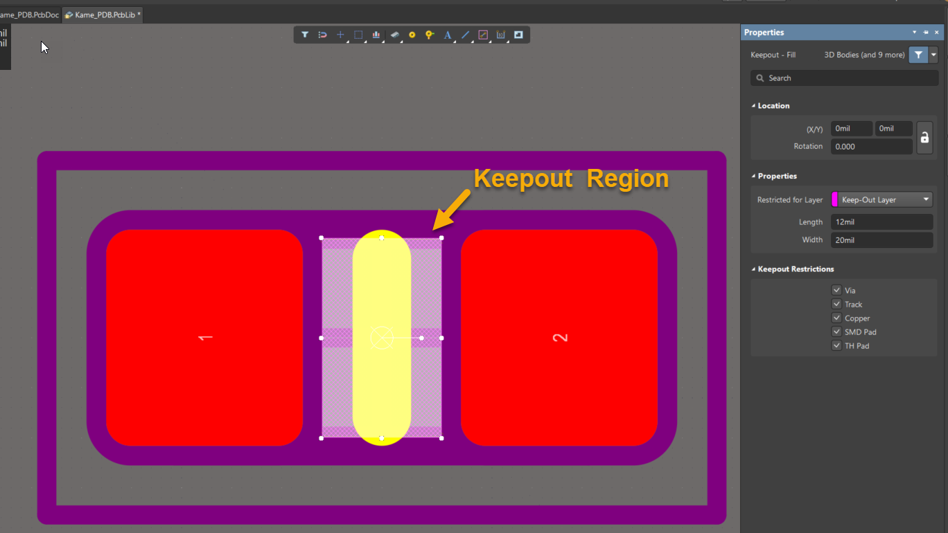
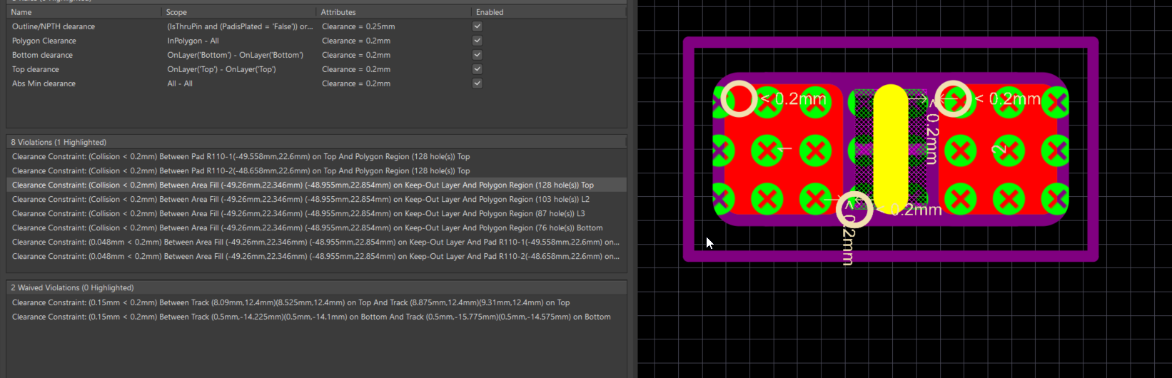
Conflict Between Keepout and Pad/Fill Regions
Some components include Keepout areas within their SMD pads to prevent copper pouring between them. However, placing these components on the PCB can trigger errors due to overlapping Keepout and Pad or Fill regions within the same footprint.
Why the Error Occurs
The Keepout region applies clearance rules globally across the PCB. When a Keepout is placed within a footprint, it conflicts with nearby Pads or Fills, triggering violations. Adjusting the Keepout clearance globally is not viable, as it would affect unrelated areas of the board.
What to Do
To avoid this issue, consider one of the following solutions:
- Use Room Definition Rules to locally override clearance values for Keepout regions.
- Replace Keepout Regions with Polygon Pour Cutouts within the footprint.
How to Do It
Solution 1: Room Definition Rule with Custom Clearance
1. Create a room that encompasses the footprint, including the Keepout, SMD Pads, and Fill regions.
2. Define a rule for this room that sets the Keepout clearance to zero for Pads and Fills.
3. Copy and paste the Keepout region into the footprint’s Keepout area.
4. Apply the rule to ensure no violations occur within the room.
Please look at the documentation link below for the room definition rule.
How to Use Rooms with Rules in Altium Designer
https://www.youtube.com/watch?v=21y-bievm5A
Solution 2: Use Polygon Pour Cutouts
1. Instead of defining Keepout regions, use Polygon Pour Cutouts within the footprint.
2. Place the cutout between the SMD pads to prevent copper pouring.
3. Ensure the cutout shape matches the intended Keepout area.
Documentation reference:
Polygon Pour Cutout Documentation
Additional Notes
There is an active feature request to improve Keepout behavior at the footprint level. You can support this enhancement by voting here:
Feature Request