
KB: How-To restrict what schematic components are transferred to the PCB
Solution Details
Schematic Compile Mask Overview
The schematic compile mask directive can be used to hide an area of the design from the compiler. This is often used to prevent error checking for circuitry that may not yet be complete. The schematic compile mask can therefore be used to hide components from the compiler, and prevent the compile masked components from being transferred to the PCB when updated.
Placing the Compile Mask
To place a compile mask in the schematic editor:
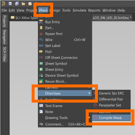
1. From the schematic editor main menu, select Place >> Directives >> Compile Mask.
2. A cross-hair will become attached to the mouse-pointer indicating the command is active.
3. Position the mouse-pointer and left-click to anchor the first corner of the compile mask.
4. Move the mouse-pointer to the diagonally opposite corner of the required (rectangular) compile mask region and left-click to anchor this second corner.
5. Either continue placing further compile masks, or right-click to exit placement mode.
Enabling and Disabling the Compile Mask
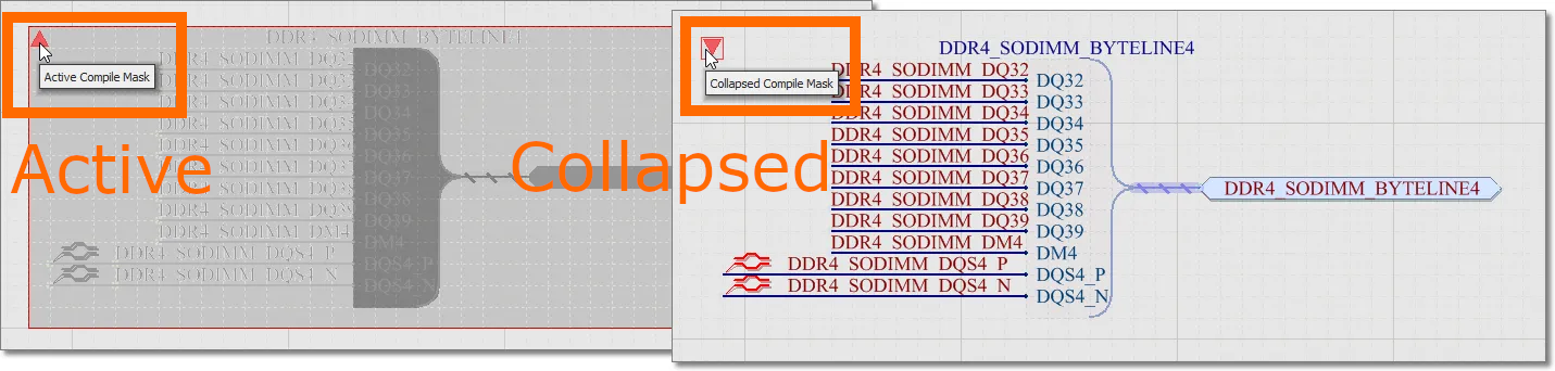
Compile masks can be toggled between active and collapsed states:
- A compile mask can be active (full frame) or collapsed (boxed triangle).
- When active (full frame) the compile mask will mask the objects underneath it.
- When collapsed (boxed triangle) the compile mask will be disabled.
- Therefore the compile mask does not need to be deleted and replaced, it can simply be expanded/collapsed as required.
Updating the PCB Document
To update the PCB after placing a compile mask:
1. From the schematic editor main menu, select Design >> Update PCB Document <file-name>.PcbDoc.
2. In the Engineering Change Order dialog click the Execute Changes button, then click the Close button.
3. All components except those underneath the compile mask should be added to the PCB document.
Additional Notes
A schematic compile mask will hide from the compiler everything underneath it, this includes net information. If the net information in the masked section of circuit is not required at the present stage of PCB layout, the compile mask method is very expedient. If the net information is important, then this method may not be amenable. A fuller solution would be to update the PCB with the entire design, and to use other available functionality to assist with the PCB layout component positioning. Positioning commands are accessible from the PCB editor main menu Tools >> Component Placement. These component placement commands hinge on the components being selected prior to running the required command. Component selection can be made in a number of ways, including: using Cross Select Mode and group selecting schematic parts; or, using the PCB panel in Components mode and selecting Component Classes.