
KB: Can we Create and Edit footprint with Altium Designer SE license
Solution Details
The Altium Designer SE license is primarily for schematic editing. However, users have raised concerns about whether this license permits PCB footprint creation and editing. Specifically, options such as placing pads or vias appear greyed out, leading to confusion about feature availability.
License Feature Limitation
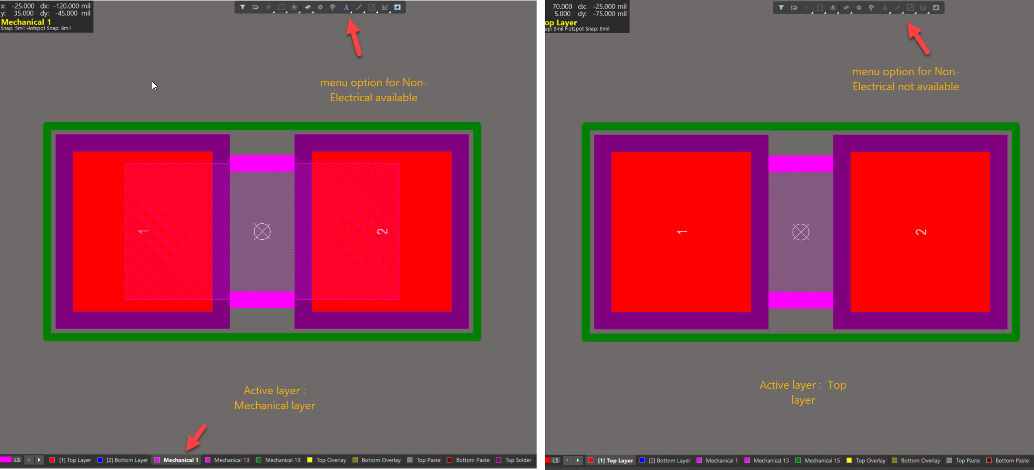
The SE license is designed for systems engineers focused on schematic capture and does not include full PCB library editing capabilities. It restricts the placement of copper objects and editing on electrical layers. When an electrical or copper layer (e.g., Top Layer) is active, related menu options are disabled. These options become available only when working on non-electrical layers such as Solder or Mechanical layers.
Available Workarounds and Options
To work within the limitations of the SE license:
- Users can perform limited edits on existing PCB libraries using non-electrical layers.
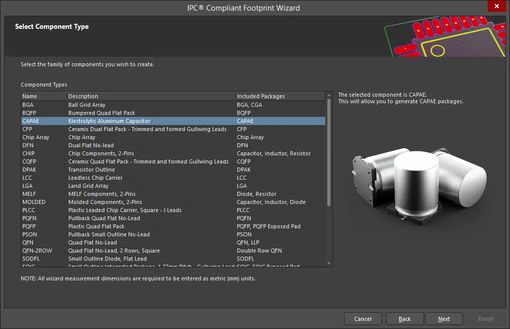
- The IPC Footprint Wizard can be used to create new footprints.
- For full editing capabilities, including unrestricted footprint creation and copper object placement, upgrading to the full Altium Designer license is recommended.
Steps to Implement the Workaround
1. Enable Object Placement on Non-Electrical Layers
1. Switch the active layer to a non-electrical layer such as Solder or Mechanical.
2. This will activate menu options for placing non-electrical objects like lines and text.
2. Create a New Footprint Using IPC Footprint Wizard
1. Open the IPC Footprint Wizard
2. Follow the wizard steps to define and generate a compliant footprint.
3. Upgrade for Full Capabilities
- Contact your Altium Account Manager to discuss upgrading to the full Altium Designer license.
Additional Notes
- Editing on electrical layers is not supported under the SE license and will consistently show disabled options.
- The IPC Footprint Wizard provides a guided method to create footprints without needing full PCB library access.